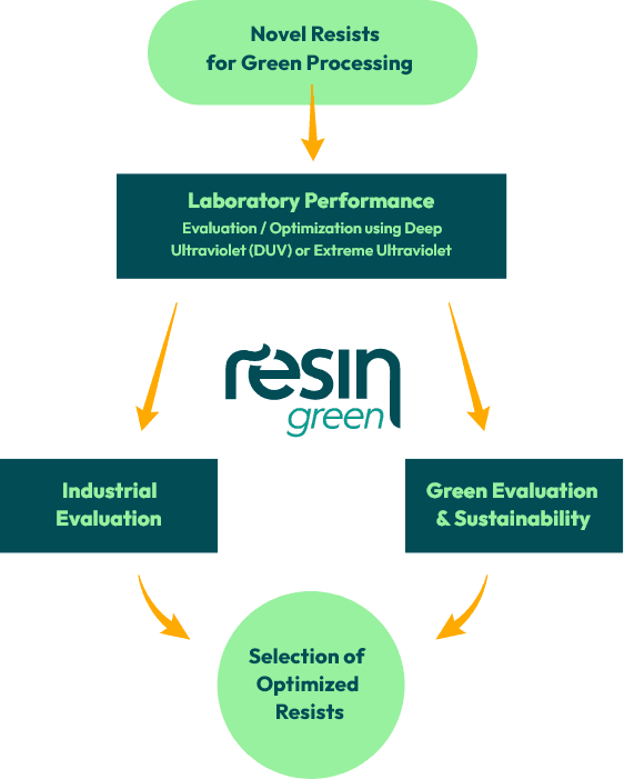

- Design and develop new green materials for the semiconductor industry following three approaches. We will evaluate these approaches targeting resist materials for both UV and EUV lithography domains, with performance characteristics suitable for the semiconductor industry.
- Demonstrate performance towards industrial viability of the concept for resists with substantially greener processing requirements compared to the current resists used in semiconductor manufacturing.
- Evaluate and quantify the expected green outcome from the use of the new resist platforms that will be developed.
- Suggest evaluation criteria for selecting resists based on combination of industrial performance at laboratory level and green processing related benefits.
Materials for a greener digital future
Developing resist materials and nanometrology methods to reduce the environmental footprint of digital technology
About the project
RESIN GREEN proposes the development of new resist material platforms which can be processed under conditions that offer clear advantages regarding the reduction of their environmental footprint.
In particular, new resist chemistries target materials that can be processed (deposited and developed) using environmentally friendly solvents such as water, very dilute aqueous base solutions, or green organic solvents.
Our Contribution
In this context, we will develop new resist materials to eliminate the use of organic solvents and aqueous alkaline solutions currently used in the lithographic process at the semiconductor manufacturing industry.
The lithographical process steps that demand the significant amounts of solvents are the spin coating solution of the photoresist as well as the development process. We target to replace the standard organic solvents used in spin coating and the highly alkaline TMAH solutions used in development with water. Greener organic solvents and very dilute basic developers will only be considered if necessary for meeting high-performance requirements.
We aim to investigate bio-source materials and new photoresist platforms suitable for exposure at 193 nm, 248 nm or EUV and achieve significant breakthroughs by designing a complete process using renewable resources and neither organic solvent nor hazardous chemicals. In addition, e-beam lithography will be considered, especially for evaluating the high-resolution potential of the proposed resist materials.
Main output
The main output of the project will be the development of:
More specifically, RESIN GREEN aims to replace the toxic materials used in lithography with bio-sourced polymers like chitosan or other polymers soluble in water-based solutions.
A well-elaborated metrology strategy with innovative aspects will be derived to characterize the quality of resist patterns, at the high-resolution domain. The metrological approaches that will be utilized, are going to be either based on data acquired by Scanning Electron Microscopy (SEM) or Atomic Force Microscopy (AFM). One of the main challenges of SEM metrology is accuracy, so towards this end, metrology will be empowered with advanced computational methods, including Machine Learning (ML) techniques, dedicated to tackling factors that affect accuracy, such as the presence of noise to meet the requirements for <1nm accuracy. In the case of AFM metrology, ML techniques will be developed to quantify and subtract tip effects in specific AFM measurements of resist patterns.
A methodology will be developed to quantify the expected green outcome from using the new resist platforms based on the Life Cycle Analysis data collection and related ISO standards. Furthermore, evaluation criteria will be elaborated for selecting resists combining green processing-related benefits with laboratory-level industrial performance.
Target Groups
-
Industry
-
Academia
-
General Public
Basic Objectives

The Challenge

The global semiconductor market, with a size of 527.88 billion dollars in 2021, is one of the most profitable and largest ones that influences several digital and emerging technologies such as automotive, computers, tablets, telecommunications, etc. Unfortunately, the semiconductor manufacturing process entails a lot of toxic materials.
Semiconductor facilities use multiple liquids and solvents such as acidic, alkaline and others that can be as hard on human physiology as they are on the materials they treat. Aside from being caustic, many commonly used chemicals are known as human carcinogens. Some examples that can carry high risk are toluene, acetone, methylene chloride, xylene, chloroform, and isopropyl alcohol.
RESIN GREEN aims to develop green and environmentally friendly materials with high efficiency for photolithography, one of the most critical steps of the semiconductor manufacturing process. It is expected that by the end of the project, we will have developed three green materials in TRL 4 with high sensitivity, low line edge roughness, and high resolution. The aforementioned technologies will be exploited almost directly by the industry, taking into consideration that STMicroelectronics is already a partner in the consortium, and ASML has already expressed interest.
Resin Green Methodology